The Basics
Once you have acquired the tutorial files you should see the following Chisel tutorial directory structure under $TUT_DIR:
chisel-tutorial/
  build.sbt # project description
  run-examples.sh   # shell script to execute one or more examples
  run-problem.sh    # shell script to execute one or more problems
  run-solution.sh   # shell script to execute one or more solutions
  src/
    main/
      scala/
        examples/   # chisel examples
          Accumulator.scala ...
        problems/   # skeletal files for tutorial problems
          Counter.scala ...
        solutions/  # solutions to problems
          Counter.scala ...
    test/
      resources/
        in.im24
        in.wav
     scala/
        examples/   # examples testers
          Adder.scala ...
        problems/   # problems testers
          Accumulator.scala ...
        solutions/  # solutions testers
          Accumulator.scala ...
        util/
          TutorialRunner.scala
Chisel source files are distributed between examples, problems, and solutions directories.
The tutorial contains the files that you will be modifying under problems/ while the solutions/ folder contains the reference implementations for each of the problems.
The folder examples/ contains source to the complete examples given in this tutorial.
Finally, the build.sbt file contains the build configuration information used to specify what version of Chisel to make your project with.
In this section, we explain how to run your first build to explore what Chisel has to offer. We will go through a simple example for a GCD module and familiarize ourselves with the source files, simulation, and Verilog generation. More comprehensive details will follow in subsequent sections of the tutorial.
Now that you are more familiar with what your Chisel directory structure contains, let's start by exploring one of the Chisel files.
Change directory into the src/main/scala/examples/ directory and open up the GCD.scala file with your favorite text editor.
You will notice that file is already filled out for you to perform the well known GCD algorithm and should look like:
// See LICENSE.txt for license details.
package examples

import chisel3._


class GCD extends Module {
  val io = IO(new Bundle {
    val a  = Input(UInt(16.W))
    val b  = Input(UInt(16.W))
    val e  = Input(Bool())
    val z  = Output(UInt(16.W))
    val v  = Output(Bool())
  })
  val x  = Reg(UInt())
  val y  = Reg(UInt())
  //in chisel2.2 tutotial use: when   (x > y) { x := x - y }  unless   (x > y) { y := y - x }
  when   (x > y) { x := x - y }
    .elsewhen (x <= y) { y := y - x }
  when (io.e) { x := io.a; y := io.b }
  io.z := x
  io.v := y === 0.U
}
The first thing you will notice is the import chisel3._ declaration; this imports the Chisel library files that allow us to leverage Scala as a hardware construction language.
After the import declarations you will see the Scala class definition for the Chisel component you are implementing.
You can think of this as almost the same thing as a module declaration in Verilog.
Next we see the I/O specification for this component in the val io = IO(new Bundle{...}) definition.
You will notice that the bundle takes several arguments as part of its construction, each with a specified type (UInt, Bool, etc.), a bit width, and wrapped into a direction (either Input or Output).
If a bit width is not specified, Chisel will infer the appropriate bit width for you (in this case default to 1).
The io Bundle is essentially a constructor for the component interface.
The next section of code performs the actual GCD computation for the module.
The register declarations for x and y tell Chisel to treat x and y as registers of type UInt().
val x = Reg(UInt()) // declares x as UInt register
val y = Reg(UInt()) // declares y as UInt register
The when statement tells Chisel to perform the operation when the condition is true.
In hardware this is basically a multiplexer selecting the values in the when block
when the condition is true, otherwise selecting the default assignment or keep a register value.
With an register on the left hand side of the expression, the assignment is executed
on a positive clock edge if the condition is true.
This is similar to how Verilog uses always @ (posedge clk) to specify synchronous logic.
Finally we see the output assignments for the computation for io.z and io.v.
One particular thing to notice is that, we do not have to specify the width of x and y in this example.
This is because Chisel does the bit width inference for you and sets these values to their appropriate widths based on the computations they are executing.
Now that we are familiar with the Chisel code for the GCD.scala file, let's try to simulate it by using the tester and the firrtl interpreter.
First, have a look at the Chisel code in src/test/scala/examples/GCDTests.scala.
This contains a Chisel implementation of a PeekPokeTester and a tester driver which will arrange to simulate the circuit, connect it to the tester, and run the tester on the simulated circuit.
The tester uses poke to drive the circuit's inputs, step to run the circuit for a single cycle, and expect to verify its output.
Change back to the root directory of the tutorials (the directory containing the file build.sbt and the run-examples.sh shell script), and invoke the run-examples.sh shell script with the name of the example circuit to be simulated:
./run-examples.sh GCDThis will generate the firrtl description of the circuit for the component defined in src/main/scala/examples/GCD.scala and use the firrtl interpreter to simulate it using the test harness defined in src/test/scala/examples/GCDTests.scala.
If the simulation succeeds, you should see some debug output followed by:
RAN 5 CYCLES PASSED
Tutorials passing: 1
[success] Total time: 2 s, completed Sep 16, 2016 10:15:32 AM
In addition to the debug output, the build also creates a test_run_dir/examples/GCD/GCD.fir file, containing the firrtl definition of the GCD circuit and its tester.
We will talk about this more later.
One of the most powerful features of Chisel is its ability to generate FPGA and ASIC Verilog from the Scala sources that you use to construct a circuit. To do this, we use an environment variable to specify a different tester backend:
./run-examples.sh GCD --backend-name verilatorThis will instruct the tester driver to generate Verilog output and use Verilator to generate a C++ simulation from the generated Verilog for the specified Chisel component.
When the Verilog generation finishes, you should see a [success] message similar to the one you saw after running the firrtl-interpreter backend.
If you look in the test_run_dir/examples/GCD/ directory, you will see quite a few additional files, notably:
- GCD.v - Verilog representation of the Chisel circuit,
- GCD.vcd - waveform dump of the circuit signals during the simulation.
The Verilog source is roughly divided into three parts:
- Module declaration with input and outputs
- Temporary wire and register declaration used for holding intermediate values
- Register assignments in
always @ (posedge clk)
You can use gtkwave to view the vcd dump.
Constructing combinational logic blocks in Chisel is fairly straightforward; when you declare a val in Scala, it creates a node that represents the data that it is assigned to.
As long as the value is not assigned to be a register type (explained later), this tells the Chisel compiler to treat the value as wire.
Thus any number of these values can be connected and manipulated to produce the value that we want.
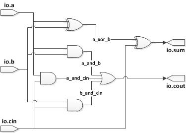
Suppose we want to construct a single full adder.
A full adder takes two inputs a and b, and a carry in cin and produces a sum and carry out cout.
The Chisel source code for our full adder will look something like:
class FullAdder extends Module {
  val io = IO(new Bundle {
    val a    = Input(UInt(1.W))
    val b    = Input(UInt(1.W))
    val cin  = Input(UInt(1.W))
    val sum  = Output(UInt(1.W))
    val cout = Output(UInt(1.W))
  })
  // Generate the sum
  val a_xor_b = io.a ^ io.b
  io.sum := a_xor_b ^ io.cin
  // Generate the carry
  val a_and_b = io.a & io.b
  val b_and_cin = io.b & io.cin
  val a_and_cin = io.a & io.cin
  io.cout := a_and_b | b_and_cin | a_and_cin
}
where cout is defined as a combinational function of inputs a, b, and cin.
You will notice that in order to access the input values from the io bundle, you need to first reference io since the input and output values belong to the io bundle.
The |, &, and ^ operators correspond to bitwise OR, AND, and XOR operations respectively.
The corresponding wires for each of these values is shown below in Figure Full Adder Circuit.
You will notice that each val corresponds to exactly one of the wires.
If you don't explicitly specify the width of a value in Chisel, the Chisel compiler will infer the bit width for you based on the inputs that define the value.
Notice in the FullAdder definition, the widths for a_xor_b, a_and_b, b_and_cin, and a_and_cin are never specified anywhere.
However, based on how the input is computed, Chisel will correctly infer each of these values are one bit wide since each of their inputs are the results of bitwise operations applied to one bit operands.
A quick inspection of the generated Verilog shows these values are indeed one bit wide:
module FullAdder(
  input   clk,
  input   reset,
  input   io_a,
  input   io_b,
  input   io_cin,
  output  io_sum,
  output  io_cout
);
  wire  a_xor_b;
  wire  T_5;
  wire  a_and_b;
  wire  b_and_cin;
  wire  a_and_cin;
  wire  T_6;
  wire  T_7;
  assign io_sum = T_5;
  assign io_cout = T_7;
  assign a_xor_b = io_a ^ io_b;
  assign T_5 = a_xor_b ^ io_cin;
  assign a_and_b = io_a & io_b;
  assign b_and_cin = io_b & io_cin;
  assign a_and_cin = io_a & io_cin;
  assign T_6 = a_and_b | b_and_cin;
  assign T_7 = T_6 | a_and_cin;
endmodule
Suppose we change the widths of the FullAdder to be 2 bits wide each instead such that the Chisel source now looks like:
class FullAdder extends Module {
  val io = IO(new Bundle {
    val a    = Input(UInt(2.W))
    val b    = Input(UInt(2.W))
    val cin  = Input(UInt(2.W))
    val sum  = Output(UInt(2.W))
    val cout = Output(UInt(2.W))
  })
  // Generate the sum
  val a_xor_b = io.a ^ io.b
  io.sum := a_xor_b ^ io.cin
  // Generate the carry
  val a_and_b = io.a & io.b
  val b_and_cin = io.b & io.cin
  val a_and_cin = io.a & io.cin
  io.cout := a_and_b | b_and_cin | a_and_cin
}
As a result, the Chisel compiler should infer each of the intermediate values a_xor_b, a_and_b, b_and_cin, and a_and_cin are two bits wide. An inspection of the Verilog code correctly shows that Chisel inferred each of the intermediate wires in the calculation to be 2 bits wide.
module FullAdder(
  input   clk,
  input   reset,
  input  [1:0] io_a,
  input  [1:0] io_b,
  input  [1:0] io_cin,
  output [1:0] io_sum,
  output [1:0] io_cout
);
  wire [1:0] a_xor_b;
  wire [1:0] T_5;
  wire [1:0] a_and_b;
  wire [1:0] b_and_cin;
  wire [1:0] a_and_cin;
  wire [1:0] T_6;
  wire [1:0] T_7;
  assign io_sum = T_5;
  assign io_cout = T_7;
  assign a_xor_b = io_a ^ io_b;
  assign T_5 = a_xor_b ^ io_cin;
  assign a_and_b = io_a & io_b;
  assign b_and_cin = io_b & io_cin;
  assign a_and_cin = io_a & io_cin;
  assign T_6 = a_and_b | b_and_cin;
  assign T_7 = T_6 | a_and_cin;
endmoduleUnlike Verilog, specifying a register in Chisel tells the compiler to actually generate a positive edge triggered register. In this section we explore how to instantiate registers in Chisel by constructing a shift register.
In Chisel, when you instantiate a register there are several ways to specify the connection of the input to a register.
As shown in the GCD example, you can "declare" the register and assign what it's input is connected to in a when... block or you can simply pass the value that the register is clocking as a parameter to the register.
If you choose to pass a next value to the register on construction using the next named parameter, or the specialized register constructor RegNext, it will clock the new value every cycle unconditionally:
// Clock the new register value on every cycle
val y = io.x
val z = RegNext(y)
If we only want to update if certain conditions are met we use a when block to indicate that the registers are only updated when the condition is satisfied:
// Clock the new register value when the condition a > b
val x = Reg(UInt())
when (a > b) { x := y }
.elsewhen ( b > a) {x := z}
.otherwise { x := w}
It is important to note that when using the conditional method, the values getting assigned to the input of the register match the type and bitwidth of the register you declared. In the unconditional register assignment, you do not need to do this as Chisel will infer the type and width from the type and width of the input value.
The following sections show how these can be used to construct a shift register.
Suppose we want to construct a basic 4 bit shift register that takes a serial input in and generates a serial output out.
For this first example we won't worry about a parallel load signal and will assume the shift register is always enabled.
We also will forget about the register reset signal.
If we instantiate and connect each of these 4 registers explicitly, our Chisel code will look something like:
class ShiftRegister extends Module {
  val io = IO(new Bundle {
    val in  = Input(UInt(1.W))
    val out = Output(UInt(1.W))
  })
  val r0 = RegNext(io.in)
  val r1 = RegNext(r0)
  val r2 = RegNext(r1)
  val r3 = RegNext(r2)
  io.out := r3
}
If we take a look at the generated Verilog, we will see that Chisel did indeed map our design to a shift register. One thing to notice is that the clock signal and reset signals are implicitly attached to our design.
module ShiftRegister(input clk, input reset,
    input  io_in,
    output io_out);

  reg[0:0] r3;
  reg[0:0] r2;
  reg[0:0] r1;
  reg[0:0] r0;

  assign io_out = r3;
  always @(posedge clk) begin
    r3 <= r2;
    r2 <= r1;
    r1 <= r0;
    r0 <= io_in;
  end
endmoduleAs mentioned earlier, Chisel allows you to conditionally update a register (use an enable signal) using the when, .elsewhen, .otherwise block.
Suppose we add an enable signal to our shift register, that allows us to control whether data is shift in and out on a given cycle depending on an enable input signal.
The new shift register now looks like:
class ShiftRegister extends Module {
  val io = IO(new Bundle {
    val in     = Input(UInt(1.W))
    val enable = Input(Bool())
    val out    = Output(UInt(1.W))
  })

  val r0 = Reg(UInt())
  val r1 = Reg(UInt())
  val r2 = Reg(UInt())
  val r3 = Reg(UInt())

  when (io.enable) {
    r0 := io.in
    r1 := r0
    r2 := r1
    r3 := r2
  }
  io.out := r3
}
Notice that it is not necessary to specify an .otherwise condition as Chisel will correctly infer that the old register value should be preserved otherwise.
Chisel allows you to specify a synchronous reset to a certain value by specifying an additional parameter when you first declare them.
In our shift register, let's add a reset capability that resets all the register values to zero synchronously.
To do this we need to provide our register declarations a little more information using the init parameter,
or using the specialized constructor RegInit, with what value we want on a synchronous reset:
class ShiftRegister extends Module {
  val io = IO(new Bundle {
    val in     = Input(UInt(1.W))
    val enable = Input(Bool())
    val out    = Output(UInt(1.W))
  })
  // Register reset to zero
  val r0 = RegInit(0.U(1.W))
  val r1 = RegInit(0.U(1.W))
  val r2 = RegInit(0.U(1.W))
  val r3 = RegInit(0.U(1.W))
  when (io.enable) {
    r0 := io.in
    r1 := r0
    r2 := r1
    r3 := r2
  }
  io.out := r3
}
Notice that reset value can actually be any value, simply replace the zeros and width to appropriate values.
Chisel also has an implict global reset signal that you can use in a when block.
The reset signal is conveniently called reset and does not have to be declared, but in order to treat it as a Bool, you need to add the toBool cast.
The shift register using this implict global reset now looks like:
class ShiftRegister extends Module {
  val io = IO(new Bundle {
    val in     = Input(UInt(1.W))
    val enable = Input(Bool())
    val out    = Output(UInt(1.W))
  })
  val r0 = Reg(UInt())
  val r1 = Reg(UInt())
  val r2 = Reg(UInt())
  val r3 = Reg(UInt())
  when(reset.toBool) {  // interpret reset as a Bool
    r0 := 0.U
    r1 := 0.U
    r2 := 0.U
    r3 := 0.U
  } .elsewhen(io.enable) {
    r0 := io.in
    r1 := r0
    r2 := r1
    r3 := r2
  }
  io.out := r3
}
This will generate slightly different looking Verilog source code but will still function the same as the previous implementation of the shift register with reset.
The following exercises can be found in your
$TUT_DIR/src/main/scala/problems/ folder. You will find that some parts of
the tutorial files have been completed for you and the section that
you need to complete is indicated in the file. The
solutions to each of these exercises can be found in the
$TUT_DIR/src/main/scala/solutions/ folder.
The first tutorial problem is to write a sequential circuit that sums in values.
You can find the template in $TUT_DIR/src/main/scala/problems/Accumulator.scala including a stubbed out version of the circuit:
class Accumulator extends Module {
  val io = IO(new Bundle {
    val in  = Input(UInt(1.W))
    val out = Output(UInt(8.W))
  })

  // flush this out ...

  io.out := 0.U
}
and a complete tester that confirms that you have successfully designed the circuit in $TUT_DIR/src/test/scala/problems/Accumulator.scala.
Run:
./run-problem.sh AccumulatorThis should fail until you complete the circuit implementing the accumulator.
Edit the src/main/scala/problems/Accumulator.scala source file and execute the run-problem.sh shell script until your circuit passes the tests.
Prev (Chisel Installation) Next (Basic Types and Operations)